XJTU team reveals electric-field-driven deformation mechanisms

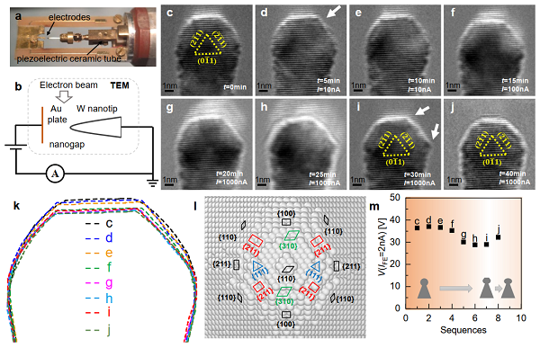
Deformation dynamics of a 3-nm curvature radius tungsten needle (cathode) under field emission.
As equipment and devices such as particle accelerators, vacuum circuit breakers, and micro/nanoelectronic devices evolve towards more complex application scenarios, miniaturized scales, and extreme electric field tolerances, insulation failure triggered by vacuum breakdown has become a critical bottleneck limiting their development.
Recent research has discovered a strong correlation between vacuum breakdown strength and a material's crystal structure and dislocation mobility, indicating that the macroscopic breakdown process originates at the microscopic scale.
In practical vacuum insulation systems, electrode surfaces inevitably possess local weak spots, such as nanoscale protrusions. These nanostructures induce localized field enhancement and field emission under strong electric fields, easily leading to breakdown.
Therefore, studying the evolutionary behavior of nanoscale protrusions on electrode surfaces under strong electric fields and their impact on field emission and insulation stability is essential for optimizing vacuum insulation structures and enhancing reliability.
In light of this, Professor Meng Guodong's team from the School of Electrical Engineering and the State Key Laboratory of Electrical Insulation and Power Equipment at Xi'an Jiaotong University (XJTU), in collaboration with Professor Shan Zhiwei's team from the School of Materials Science and Engineering at XJTU and Professor Flyura Djurabekova's team from the University of Helsinki, proposed a research method combining in-situ electrical measurements with microscopic morphology characterization using transmission electron microscopy (TEM). They studied the deformation behavior of pure tungsten nanoelectrodes with different curvature radii (R = 3 nm, 5 nm, 9 nm) under field emission (~GV/m).
The research revealed the microscopic structural evolution law of nanoelectrodes under the coupled action of strong electric fields and field emission, exhibiting significant size dependence and crystal plane correlation: Electrodes with small curvature radii (R = 3 nm, 5 nm) followed a deformation path of spherical-Wulff polyhedron-spherical under the combined action of high electric fields and field emission currents, and a significant dislocation nucleation, diffusion, and annihilation process was observed in the 5-nm tip.
Furthermore, by analyzing the thermal effects of field emission and the Maxwell stress, and by designing counter-polarity control experiments, they decoupled the electron wind effect from the electric field effect, revealing that the electron wind effect and its induced field-assisted evaporation constitute the dominant deformation mechanism.
This study, for the first time, reveals from an experimental perspective the electrostatic damage characteristics and dominant mechanism of metallic nanoelectrodes under strong electric fields and field emission conditions, providing important experimental evidence and theoretical support for promoting the insulation structure design and reliability optimization of high-performance electrical equipment and micro/nanoelectronic devices.
This research has been published in the internationally renowned journal Nature Communications under the title Unveiling Electric-Field-Driven Deformation Dynamics in Metal Nanostructures.
-

XJTU holds 2026 New Year Concert
December 30, 2025
